The article A simple Simsmith model for exploration of a common EFHW transformer design – 2t:14t proposed a simple model.
The previous proposal
![]()
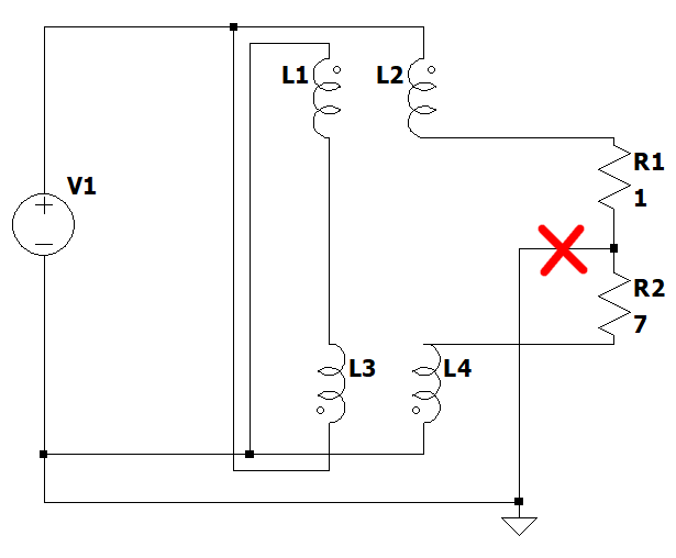
Above is the equivalent circuit used to model the transformer. The transformer is replaced with an ideal 1:n transformer, and all secondary side values are referred to the primary side.
The model works quite well for low leakage inductance / low ratio transformers but falls down for the higher leakage inductance / higher ratio transformers.
An improved model
The improved model is similar, but Cse in the model above is distributed to the outer sides of the lumped constant model.
![]()
Above is the equivalent circuit used to model the transformer. The transformer is replaced with an ideal 1:n transformer, and all secondary side values are referred to the primary side. Continue reading An improved simple Simsmith model for exploration of a common EFHW transformer designs (v1.03)