NanoVNA-H – modification of v3.3 PCB to start the bootloader from the jog switch

Later NanoVNA-H* hardware allows the device to start in bootloader mode by holding the jog switch in whilst powering on. It is a very convenient facility for firmware update, much more convenient than taking the case apart to jumper BOOT0 to VDD. (Some later firmwares provide a menu option to start the bootloader… but of course that is only useful if the firmware is running properly and may not be useful in the event of a failed firmware update.)

This was a mod I devised prior to the v3.4 hardware change, it is not identical to that change as it preceded it, but it works fine on v3.3 hardware and may work on earlier versions.
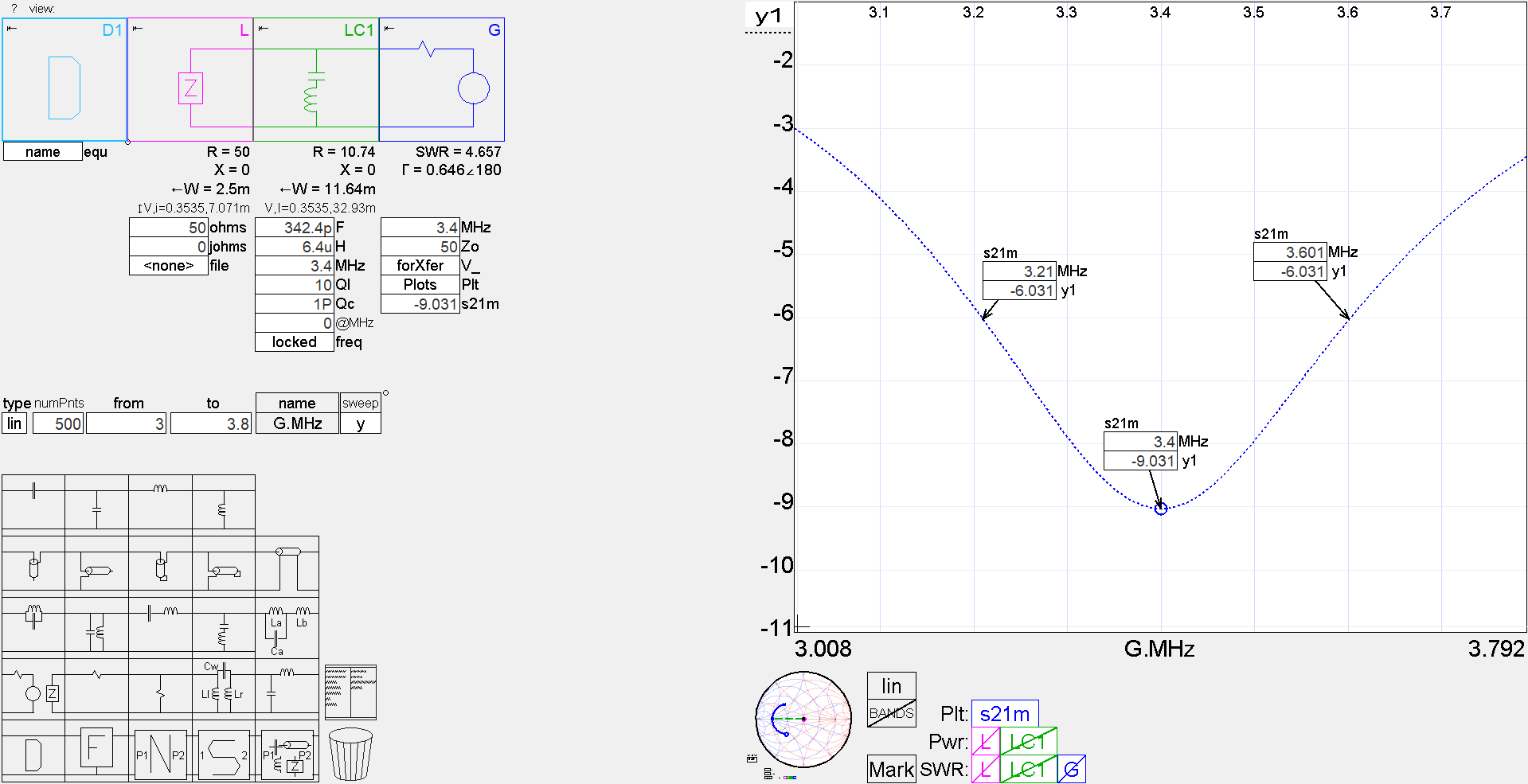
Boot switch

The mod calls for replacing R5 with a 1k (1402) and running a short jumper from the T terminal of the jog switch to the un-grounded end of R6.

To use it, hold the jog switch in and turn the nanoVNA on.

Above a pic of the mod. It is a simple mod, but very fine soldering so it might not be within everyone’s capability.

NanoVNA-H* – a howto do firmware update using STM32CubeProgrammer

One of the many solutions for updating firmware on the NanoVNA-H* is using ST’s STM32CubeProgrammer.

It would seem that STM32CubeProgrammer deprecates the older DfuSe Demo utility… which remains available for download. Some online experts have inferred that the word Demo in the latter implies it is not the full quid… but they misunderstand the context.

Windows drivers

The two are kind of incompatible in that they use difference device drivers. If you set your machine up for one, it breaks the other until you switch the correct driver in.

STM32CubeProgrammer uses libusbk (or the like) whereas DfuSe Demo uses the STub30 driver.

Above is a dump of the driver properties in my working instance. Continue reading NanoVNA-H* – a howto do firmware update using STM32CubeProgrammer

NanoVNA-H4 – battery charge from discharged

This article documents the charge cycle of a NanoVNA-H4 from fully discharged to charged.

The DUT is probably a ‘standard’ H4, but with Chinese sourced produce, you never, never know.

The original battery fitted to the NanoVNA-H v4.3 is a 804050 (8.0x40x50mm) 2000mAh LiPo pouch cell (1S) with protection board.

The charger chip is a TP4056, and it would appear to be limited by Rprog to about 0.75A (which includes the current drawn by the working NanoVNA-H4) (though the circuit employed would appear to tweak that limit between VNA on and off conditions with R44). The TP4056 is simply a charger chip, it will not prevent over-discharge of the cell so it is wise to use a cell with protection board (as originally supplied on the DUT).

Above is a plot of the calibrated battery voltage reported by the NanoVNA-H4. Continue reading NanoVNA-H4 – battery charge from discharged

Center-Fed Dipole : elements length for a Z=200 +/- 0j ohms

A chap asked online for dimensions of a 50MHz dipole with a feed point of 200+j0 to suit 50Ω feed line and a 1:4 coax half wave balun. The “+/- 0j” is hammy Sammy talk from an ‘Extra’.

This type of balun, properly implemented, is a good voltage balun, and it is quite suited to a highly symmetric antenna.

A good voltage balun will deliver approximately equal voltages (wrt the input ground) with approximately opposite phase, irrespective of the load impedance (including symmetry).

Where the load is symmetric, we can say a good voltage balun will deliver approximately equal currents with approximately opposite phase, irrespective of the load impedance.

It is an interesting application, and contrary to the initial responses on social media, there is a simple solution.

One solution

Let’s take a half wave dipole and lengthen it a little so the feed point admittance becomes 1/200-jB (or 200 || jX). We will build an NEC model of the thing in free space.

Above is a sweep of the dipole which is 3.14m long (we will talk about how we came to that length later), and the Smith chart prime centre is 200+j0… the target impedance. Continue reading Center-Fed Dipole : elements length for a Z=200 +/- 0j ohms

End Fed Half Wave matching transformer – 80-20m – model and measurement

Reviewing consistency of measured and model data, the first posting was based on an incorrect model parameter (aol), the article is now revised for the correct value, apologies.

End Fed Half Wave matching transformer – 80-20m described a EFHW transformer design with taps for nominal 1:36, 49, and 64 impedance ratios.

Keep in mind that this is a desk design of a transformer to come close to ideal broadband performance on a nominal 2400Ω load with low loss. Real antennas don’t offer an idealised load, but this is the first step in designing and applying a practical transformer.

The transformer comprises a 32t of 0.65mm enamelled copper winding on a Fair-rite 5943003801 core (FT240-43) ferrite core (the information is not applicable to an Amidon core), to be used as an autotransformer to step down a EFHW load impedance to around 50Ω. The winding layout is unconventional, most articles describing a similar transformer seem to have their root in a single flawed design, and they are usually published without meaningful credible measurement. Continue reading End Fed Half Wave matching transformer – 80-20m – model and measurement

U.FL connectors – hints

This article expands on discussion at nanoVNA – that demo board and its U.FL connectors.

Before looking at the specifics of the Hirose U.FL connector, clean connectors work better and last longer. That should not be a revelation.

A can of IPA cleaner and a good air puffer are invaluable for cleaning connectors. The air puffer show  has a valve in the right hand end, it doesn’t suck the dirt and solvent out of the connector and blow it back like most cheap Chinese puffers, this one was harder to find and expensive ($10!). Continue reading U.FL connectors – hints

NanoVNA-H4 – inductor challenge – part 7

One method described online on YouTube and in social media is the 90° method as I will call it.

The reason why people make measurements at +/- 90 degrees on the smith chart is because the measurement accuracy using the shunt configuration when trying to measure the nominal value of an inductor or capacitor is highest at 0+j50 ohms (or 0-j50 ohms… OD).

To be clear, this is the phase of s11 or Γ being + or – 90° as applicable.

Is there something optimal when phase of s11 is + or – 90°?

Does the software / firmware / hardware give significantly more accurate response under such a termination?

Above is a diagram from a HP publication, slightly altered to suit the discussion. Continue reading NanoVNA-H4 – inductor challenge – part 7

NanoVNA – measuring Q of an inductor using s21 – fails?

There is a fashion of seeing s21 measurements as the answer to all things, and amongst the revelations is an explanation of measuring inductor Q using s21 shunt through configuration.

Let’s explore the use of s21 shunt through to directly find the half power bandwidth of a series tuned circuit and calculate the Q from that and the resonant frequency (as demonstrated by online posters).

To eliminate most of the uncertainties of measurement, let’s simulate it in Simsmith.

The simulation has a series tuned circuit resonated at 3400kHz, and the source and plot are set to calculate |s21| in dB. Though the model specifies Q independent of frequency, the D block adjusts Q for a constant equivalent series resistance (ESR) which simplifies discussion of resonance and Q. Continue reading NanoVNA – measuring Q of an inductor using s21 – fails?