 |
| OwenDuffy.net |
|
*** DRAFT ***
Many PLL and DDS chips use an input circuit similar to a logic input, there are often CMOS inputs with an equivalent circuit that looks like a very small capacitance (perhaps a few pF) with some series resistance. At 10MHz, the look close enough to a few pF. That works just fine for a TTL/CMOS reference oscillator module located very close to the synthesiser chip.
This article explores what happens with an external reference source is cabled using coax using some test cases that expose what is happening.
Reference sources, eg GPS Disciplined Oscillators and Rubidium oscillators, commonly fall into two families, those with a sinusoidal output and those with a square wave output. If they are designed for use with a significant length of connecting cable, the output circuit should be designed to drive the cable.
Some reference sources may have low resistance to ground at DC, so they bias their output to be centred about 0V.
The source impedance at the fundamental and harmonics might not be tightly controlled, though some may look like a fairly ideal 50+j0Ω source at all frequencies.
They can be a mixed bag, and good synthesiser designs will control this uncertainty for predictable performance.
The example of a 10MHz symmetric square wave reference source is explored to demonstrate the issues that arise. A lossless section of 50Ω line with propagation delay of 10ns (representing about 2m of cable with velocity factor equal to 0.67) is modelled. The source impedance is chosen to be different to the cable characteristic impedance to expose the effects of a mismatched source.
|
|
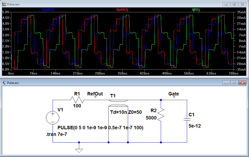
Fig 1 shows some key voltages and currents. The blue trace is the voltage at the RefOut node, the green trace is the current from the source (through the 100Ω resistor) and the red trace is the voltage appearing at the input on the synthesiser chip (Gate). The 5000Ω resistor is for demonstrating the effect of input matching and has negligible effect in this model.
The most important thing to note is the voltage appearing on the input terminal of the synthesiser chip (red). What is ideally required for low phase jitter is a reference signal that rapidly passes through the voltage range between a logic 0 and a logic 1 on the synthesiser input. That does not happen in this case.
Note too the current waveform at the reference source (green plot). This may cause undesired effects on the control loop within the source unless the output is suitably buffered. Not all reference sources effectively isolate their output terminals from the internals of the source.
Lets look at the same model with a matched termination at the load end of the cable.
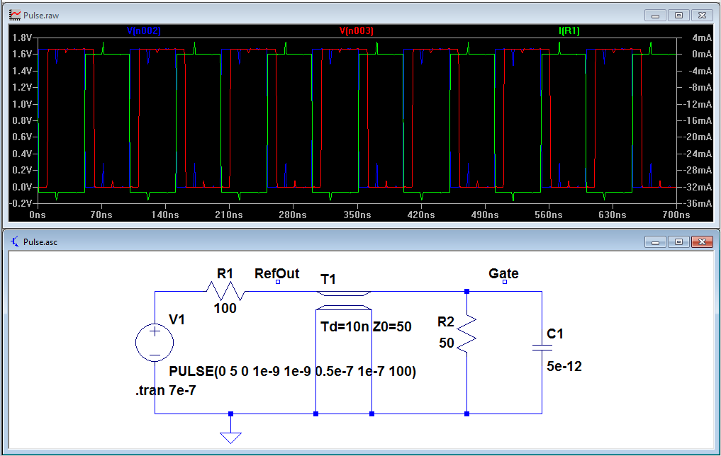 |
Fig 2 shows some key voltages and currents. The red trace is again the voltage at the synthesiser input pin. This time, the transition between a logic 0 and a logic 1, and vice versa, is fast and clean.
Of course, for reliable keying of the input terminal in this scenario, the source needs to be raised in voltage, around 15V for the 100Ω source case, or around 10V for a 50Ω source.
Some might suggest that termination of the source end will absorb any reflections and eliminate the problems.
Well, does it?
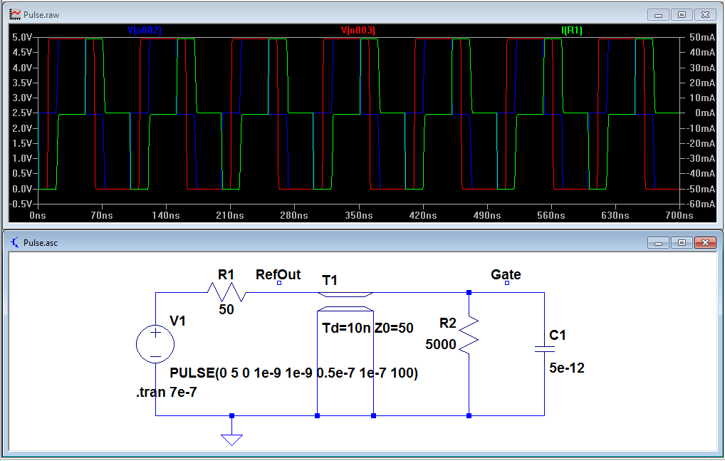 |
Fig 3 shows some key voltages and currents. The red trace is again the voltage at the synthesiser input pin. This time, the transition between a logic 0 and a logic 1, and vice versa, is fast and clean.
The weakness of this approach is that the synthesiser depends on the implementation in an external reference for good performance, whereas terminating the synthesiser input helps it to work with any external reference. Whilst the synthesiser input waveform is good, the source current waveform is not so good. Controlling the source impedance is not usually as easy as controlling the load impedance in this type of scenario.
The case with a sinusoidal source is explored, but this time with a quarter wave length of cable (5m).
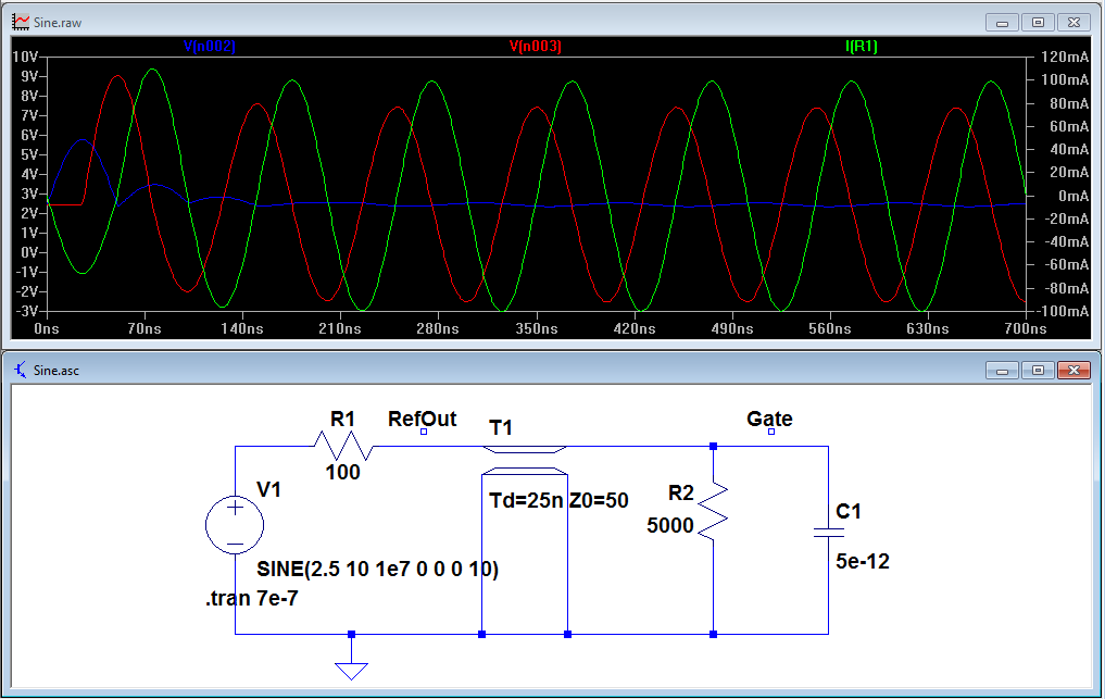 |
Fig 4 shows the waveforms for the unterminated sine wave case. In this case, the voltage at the synthesiser input transitions from logic 0 to logic one as quickly as can be expected with a sine wave.
The blue plot is interesting, it shows the voltage at the reference out terminals, and it can be seen to be much lower than that at the load end of the cable. This is a result of the very high VSWR on the cable (>30:1).
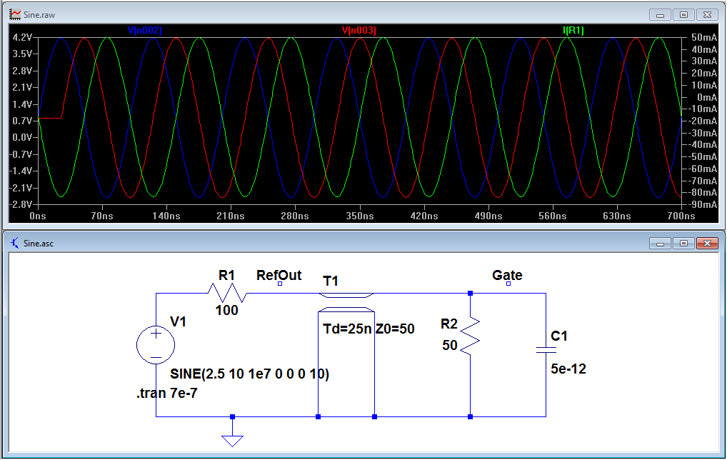 |
Fig 5 shows the case for a terminated line with sinusoidal reference.
A better approach is to put a buffer on the synthesiser input pin.
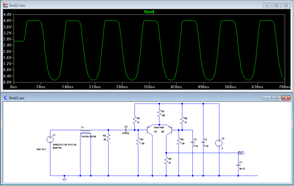 |
Fig 6 shows a simple discrete 5V buffer for driving a CMOS input pin. (The 5pF is the simulate the input pin, it is not part of the buffer circuit.)
The simulation waveform is for a -10dBm 50Ω sinusoidal source. The buffer output (green plot) transitions rapidly through the region between a logic 0 and logic 1 for best noise immunity, and the buffer input impedance terminates a 50 ohm line to minimise line reflections and adverse effects on both source and buffer.
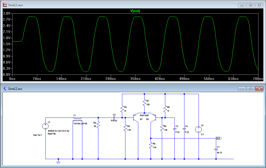 |
Fig 7 shows the same circuit biased for a 3.3V supply.
The voltage appearing at a synthesiser reference clock input pin from a reference source connected by a significant length of transmission line might be adversely affected by line reflections if the line is not adequately matched at the load end. The outcome might be degraded phase jitter as a result of slow transition between states exposing the synthesiser to noise superimposed on the reference clock.
Terminating the input terminal may be an effective means of controlling line reflections and resulting poorer phase noise from the synthesiser.
| Version | Date | Description |
| 1.01 | 29/04/2012 | Initial. |
| 1.02 | ||
| 1.03 | ||
| 1.04 | ||
| 1.05 |
© Copyright: Owen Duffy 1995, 2021. All rights reserved. Disclaimer.