 |
| OwenDuffy.net |
|
*** DRAFT ***
A ham friend purchased a Wouxun KG-UV920P as his first VHF radio. He elected to buy it from a Chinese eBay seller.
A few months after purchase, it failed losing all output on all bands.
The symptoms were that there was no output into a dummy load on VHF and UHF, and in both cases the radio drew 10A key down at 13.6V.
The problem was reported to Wouxun China who advised that on the basis of those symptoms, they were confident that they knew what the problem was, and they offered to send the parts if we were prepared to install them.
A copy of the schematic or service manual was requested at least three times from Wouxun, but they silently ignored all requests.
In fact their offer was to send a 2SK3476 driver FET at no charge, but they asked for US$19+handling for shipping the part which would weigh less than 1g (<0.002lb)... so it wasn't really at no charge, but rather the most expensive 2SK3476 you could buy. Note that the eBay seller sent the whole radio by expedited freight from China for just US$18... so Wouxun's charges to send the FET from the factory are simply a scam!
Along with their diagnosis that the problem was entirely failure of the driver FET were details of a hardware modification to reduce the supply voltage to the driver FET from close to 13.6V to closer to 8V, presumably to reduce the heat dissipation and the incidence of failures.
They turned out to be quite correct in their diagnosis, they obviously know of a vulnerability in the driver stage of the radio.
|
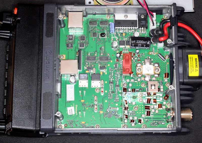
Fig 1 shows the topside of the PCB and the driver transistor is highlighted with red shading. The FET is a small surface mount package under the stainless steel saddle.
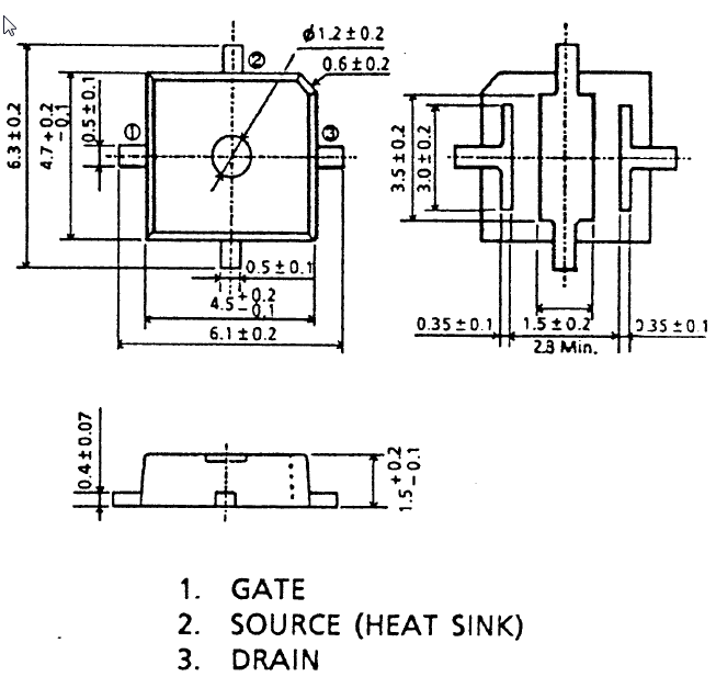 |
Fig 2 shows the FET package dimensions. Note the metallic connection for the source, it extends across the underside of the package, and this must be soldered to an adequate heat sink to achieve the required dissipation rating.
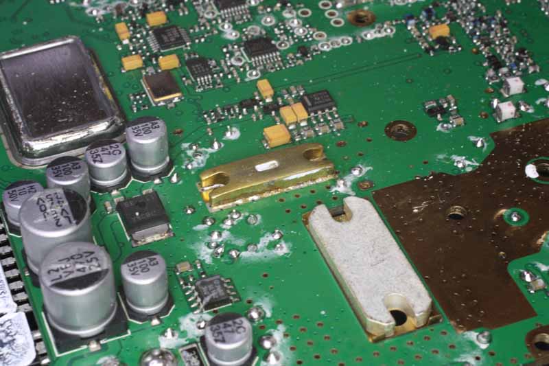 |
Fig 3 shows the detail of the underside of the driver FET. The brass bar soldered to the underside of the board projects through a rectangular opening in the PCB to be flush with the topside of the PCB. The FET is soldered to the top side of this brass link for thermal conductivity, and when the board is fitted to the case, thermal compound is applied to the underside of this brass thermal link to provide good thermal conductivity to the die case aluminium heat sink / case.
This method of construction presents challenges for both removal and replacement of the FET.
The old FET was removed by breaking it up, removing the parts and the topside of the board cleaned of excess solder and flux residue. It turns out that this cleaning process dislodged another component that was not properly attached, more later!
The supply modification was performed prior to installing the new FET. It was a low risk modification.
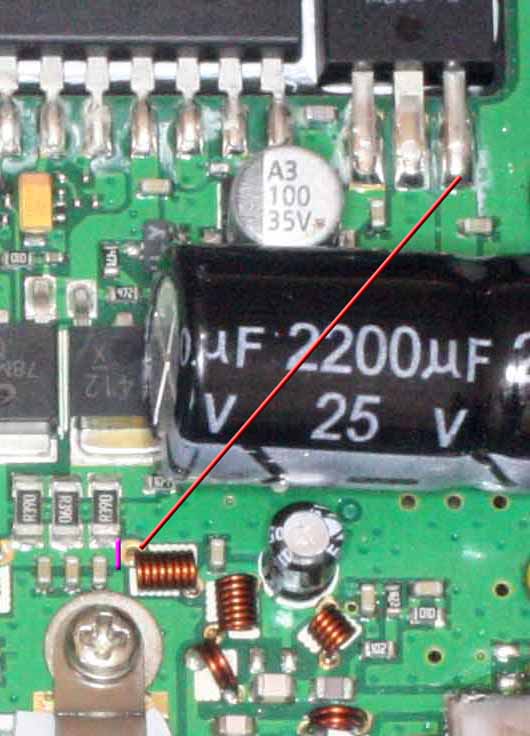 |
Fig 4 shows the modification details. The modification calls for:
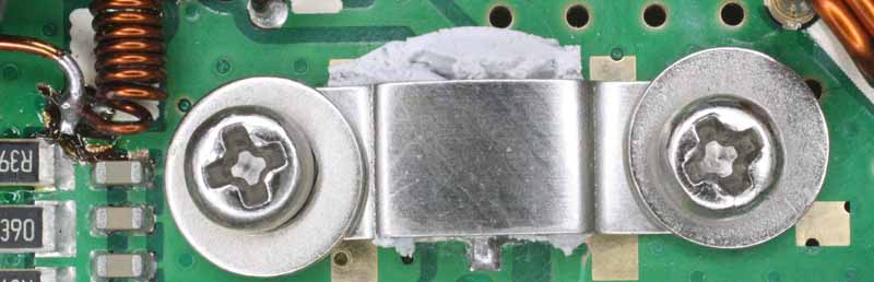 |
Fig 5 shows the modification near the driver, the track is cut between the resistors and caps and the inductor, and the inductor is wired back to the 8V regulator in the back corner of the board. Space is very tight! Make sure you have properly severed the track. Route the red wire under the large electro, but make sure you can still lay the large electro down to close the case.
Several new FETs were source on eBay, 6 for A$12 posted.
The new FET was cleaned, and a small quantity of solder paste was applied to the thermal link projection. The FET was carefully positioned and the saddle was installed with some M2.5 machine screws and nuts through the board with a little silicone wire as a compression spring under the saddle.
With the FET in the correct position (check, check and check again), and clamped against the thermal link, the board was turned upside down and a large clean soldering iron was applied to the now top of the heat link until the solder to the board had melted for a few seconds in the hope that the solder paste on the FET side would melt and solder the FET to the thermal link.
Having done this, an attempt was made to pull the FET off the PCB. It was stuck fast, the soldering operation appeared successful.
Now the four terminals were attached, and the board cleaned of flux reside with solvent, and blown clean with compressed air.
Thermal compound was applied to all the of the contact points (regulators, final FET, driver FET etc) and the board was reinstalled in the case. The driver saddle and original silicone pad were reinstalled, and everything tightened.
A thermocouple bead was clamped under one end of the saddle and in contact with the source tab on that side to sense the temperature of the FET.
The transmitter was tested on 440MHz and the temperature of the driver FET monitored to ensure that it was thermally connected to the case. It's temperature rose to 50° and the case was within a degree or so of that. Tx off, compressed air was applied to the FET which cooled quickly below the case temperature and when the air was removed, the FET warmed up the the case temperature within a couple of seconds. It appeared that the FET is properly thermally linked to the external case.
Tx output on 440MHz was 36W, a little below the specification
There was zero output on 146MHz. It was found that a component had been scrubbed off the board when cleaning the flux residue from the FET removal. Given that it was a small paintbrush used for scrubbing, the part was obviously not attached securely.
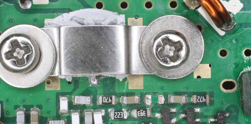 |
Fig 6 shows the area with the missing component, it is just below and to the left of the right hand screw. Note the right hand pad is copper coloured, it had clearly not soldered properly in manufacture. The left hand pad had lifted and was contacting the grounded capacitor to its left. Wouxun would not help with providing any information about the missing component, emails were ignored. Having moved the left hand tab so it was not grounded, output power was obtained on 146MHz. A small variable cap was connected to the missing part terminals and the performance was insensitive to variations. It appears to be a RF decoupling capacitor, so 100pF was installed.
If you look carefully along the bottom of Fig 6, you will see two capacitors almost touching. They are so close, it is not possible to insert a piece of paper between them. The generally poor alignment of parts with the PCB pads is a classic sign of inadequate soldering temperature, when the solder paste melts properly, surface tension pulls the components centrally over their respective pads. Poor production quality was evident in other places.
On test at 13.8V, the radio delivers 44W at 146MHz, and 36W at 440MHz. Both are a little below spec and that may be due to the reduced driver voltage, or for some other reason (including general failure to meet spec).
The radio was tested on a Motorola R2000 analyser to ensure that it worked properly and returned to my friend as working.
 |
Fig 7 shows the driver area from an earlier model (11/12) of the KG-UV920P. The driver FET looks different, and may be an RD07 as was used in the earlier 'R' model. This one appears to run the driver directly off the 13.6V supply so is likely to be susceptible to FET failure like the one discussed earlier in this article. The underside detail may be different to the model pictured earlier in this article.
Conclusions are:
Not all Wouxun radios will fail, but it appears that this radio is a flawed design. Owners may choose to perform the factory recommended modification to reduce the risk of failure.
In any event, ensure an unrestricted supply of cool air to the underside of the radio.
The transmit meter does not measure RF output voltage, and was inclined to show full scale with zero output when the driver was faulty, irrespective of the power setting. Without a circuit diagram, it is difficult to explain how it works... and so it is near useless.
| Version | Date | Description |
| 1.01 | 13/11/2013 | Initial. |
| 1.02 | ||
| 1.03 |
© Copyright: Owen Duffy 1995, 2021. All rights reserved. Disclaimer.