NanoVNA source mismatch error

One of the popular ideas online is that the correction process in the NanoVNA does not correct errors in mismatch at Port 1 and Port 2. This article deals with the first case ONLY, Port 1 mismatch.

An experiment with source VSWR nominally 2:1

A NanoVNA was configured with a SMA tee connected to Port 1 and a good 50Ω termination connected to the branch port, see the pic below. The left hand side of the tee becomes the new Port 1 interface, and by virtue of the additional 50Ω shunt termination, if the native Port 1 was indeed well represented by a Thevenin equivalent circuit with Zs close to 50+j0, the Thevenin source impedance is now closer to half that, Zs close to 25+j0.

Some would calculate this mismatch as causing a mismatch loss of 0.512dB that is additional loss in the s21 path.

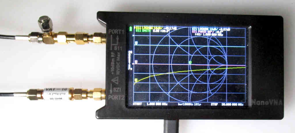
Above is the test setup. The NanoVNA was SOLT calibrated with cal parts attached to the left hand side of the tee and the 200mm coax jumper from that point to Port 2. Continue reading NanoVNA source mismatch error

Trying to make sense of Nanosaver’s R/ω and jX/ω graph

Nanosaver v0.4.0 contains a graph that I have found difficult to understand, much less find application.

Above is the graph scaled R/ω and jX/ω, and an untitled X axis, though it would appear to be frequency in Hz (scaled by the M multiplier).

I had difficulty reconciling the Y values plotted for R/ω and jX/ω with the displayed R,jX values.

David F4HTQ offers the following explanation online.

I add some explanations.

I asked Rune if he could add this graphic because it is very useful.
It display curves that have exactly the same shape as the complex permittivity curves (μ’r and μ”r) of the ferrite datasheets.

The values do not match those of the constructor curve ( to have the right value the software might know the exact geometry of the inductor) , but the shape is absolutely identical.

This allow to easy identify unknown ferrite core, and to better understand how to use it in a RF device.

He says permittivity… but he is talking about permeability.

The quote seems to say the Y axis scale is worthless?

In any event, the underlying R,X data only follows µ at frequencies well below the self resonant frequency (SRF) of the inductor.

Let’s try a measurement

Continue reading Trying to make sense of Nanosaver’s R/ω and jX/ω graph

Digital display for half wave detector with cubic spline interpolation – part 4

Digital display for half wave detector with cubic spline interpolation – part 1 and following articles laid out the design concepts of a power meter display.

Digital display for half wave detector with cubic spline interpolation – part 2 described a simple cubic spline interpolation model.

This article examines the problem a little deeper to arrive at an improved solution.

The chart above compares the response of an ideal peak detector (cyan) with an LTSPICE simulation of a BAT46 with 57kΩ load (orange x). Whilst the simulation approaches the ideal at peak RF voltage Vp greater than 3V, it departs greatly at very low Vp. Continue reading Digital display for half wave detector with cubic spline interpolation – part 4

Becen 25W type N dummy load


I purchased an inexpensive 50Ω dummy load rated at 25W from Becen on Aliexpress (~$20 inc shipping), the intended application is HF.

Above, the dummy load.

Above, the centre pin passes a gauge test, doesn’t satisfy the Precision N criteria, but well within tolerance of non-precision N connectors. Continue reading Becen 25W type N dummy load

Digital display for half wave detector with cubic spline interpolation – part 3

Digital display for half wave detector with cubic spline interpolation – part 1  and following articles laid out the design concepts of a power meter display.

Whilst the preferred target was an Arduino Zero (SAMD21G) for its 32bit architecture, speed, and 12bit ADC, the code was developed to run on a Zero or a Arduino Nano (ATmega328P).

This article explores a trial of an external ADC module using an ADS1115 chip, 4 channels 16bit +/- ADC.

Above is the prototype, Arduino Nano on the left,  the ADS1115 module is to the right of the display. Continue reading Digital display for half wave detector with cubic spline interpolation – part 3

Implementation of G5RV inverted V using high strength aluminium MIG wire – 5 year review

This article continues on from Implementation of G5RV inverted V using high strength aluminium MIG wire documenting review after 5 years operation under a wide range of temperature, humidity and wind conditions.

Above is a view of the steel mast with the Inverted V G5RV rigged from the top of the 11m mast using a halyard though a purchase on a small gibbet to offset the antenna and feed line from the mast. There are lateral guys at 7m height, and the left hand one is non-conductive synthetic fibre rope. Atop the mast is a 2m/70cm vertical. Continue reading Implementation of G5RV inverted V using high strength aluminium MIG wire – 5 year review

Digital display for half wave detector with cubic spline interpolation – part 2

Digital display for half wave detector with cubic spline interpolation – part 1 laid out the design concepts of a power meter display.

Whilst the preferred target was an Arduino Zero (SAMD21G) for its 32bit architecture, speed, and 12bit ADC, the code was developed to run on a Zero or a Arduino Nano (ATmega328P). Initially, my preferred approach of storing device calibration parameters in EEPROM was shelved because the SAMD21G does not have EEPROM, and it’s NVM alternative is not nearly as convenient.

Notwithstanding that, EEPROM support has been plumbed in and tested. For devices supporting Arduino EEPROM library, calibration coefficients can be supplied in EEPROM, or inline in source code.

The interpolation table is calculated separately in Excel (using a custom VBA function library), but could be done in any suitable tool.

Above is a screen shot  extract of the spreadsheet, the column on the right is C array initialisation code for pasting into the project source code. The same values are loaded into the EEPROM data structure if used. Continue reading Digital display for half wave detector with cubic spline interpolation – part 2

Digital display for half wave detector with cubic spline interpolation – part 1

Digital display for QRP labs 20W dummy load – part 1 and the following articles discussed an approach to compensating the non-linear response of the half wave detector by finding a polynomial curve fit over a desired range. Unfortunately, the range for a good fit can be smaller than one desires.

This article discussed an alternative using cubic spline interpolation and might be applicable to extend the range or for responses that aren’t well approximated by a simple curve fit.

Introduction

Essentially, this technique applies a piecewise polynomial to fit the data points, and a relatively small number of data points may provide a very good approximation.

The graph above shows: Continue reading Digital display for half wave detector with cubic spline interpolation – part 1

Digital display for QRP labs 20W dummy load – part 2

Digital display for QRP labs 20W dummy load – part 1 laid out a initial study into the feasibility of an approach to the project.

A prototype has been built based on an Ardunio Nano (ATmega328P 5V 16MHz). The ‘328P is loaded with a custom build of Optiboot 8 supporting reading and writing EEPROM.

Above, another prototype using a 0.96″ 128×64 OLED display, an end to end test of a BAT46 prototype for function testing using an Arduino Nano and OLED display. This prototype is well within 5% accurate based solely on the LTSPICE model, assuming no error in the voltage divider, tracking well from 1W to 20W. When calibrated for the voltage divider and ADC Vref error, power displayed was within 2% of a proven power meter at several spots from 0.8W to 25W, on a spot check it is within 10% (0.4dB) at 1mW. Continue reading Digital display for QRP labs 20W dummy load – part 2

NanoVNA-H – modification of v3.3 PCB to start the bootloader from the jog switch

Later NanoVNA-H* hardware allows the device to start in bootloader mode by holding the jog switch in whilst powering on. It is a very convenient facility for firmware update, much more convenient than taking the case apart to jumper BOOT0 to VDD. (Some later firmwares provide a menu option to start the bootloader… but of course that is only useful if the firmware is running properly and may not be useful in the event of a failed firmware update.)

This was a mod I devised prior to the v3.4 hardware change, it is not identical to that change as it preceded it, but it works fine on v3.3 hardware and may work on earlier versions.

Boot switch

The mod calls for replacing R5 with a 1k (1402) and running a short jumper from the T terminal of the jog switch to the un-grounded end of R6.

To use it, hold the jog switch in and turn the nanoVNA on.

Above a pic of the mod. It is a simple mod, but very fine soldering so it might not be within everyone’s capability.